Changes in a material's electrical conductivity
caused by its deformation can be used to sense pressure. Carbon
nanotubes offer greater sensitivity in such strain gauges.
Philip Ball
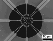
Top view of the
dimple-shaped pressure sensor, showing the electrodes connecting to a
central nanotube, which is too small to discern here. Adapted from Ref. 1. Copyright (2006) American Chemical Society.
An ultrasensitive pressure sensor that works by
bending carbon nanotubes has been made by a team of researchers in
Switzerland, Germany and the USA1.
They say that their sensor is marginally more
sensitive than the best devices currently made from micromachined
silicon — so-called microelectromechamical systems (MEMS). It works on
the principle that carbon nanotubes are piezoresistive: when they are
bent or stretched, their electrical resistance changes.
This property of carbon nanotubes has been known
for several years, and has led to speculation about whether nanotubes
could be used in strain gauges and pressure sensors. In 2000, Hongjie
Dai at Stanford University in California and his co-workers showed that
stretching a nanotube across a microscopic trench using an atomic force
microscope could alter its resistance by two orders of magnitude2.
Last year, Dai's team stuck a nanotube down onto a thin silicon nitride
membrane and showed that bending the membrane by applying pressure
could produce a significant change in the current passing through the
nanotube3.
Dai's investigations revealed that both the
magnitude and the sign of the change in resistance depend on the
precise molecular structure of the nanotube. For nanotubes with
structures that confer metallic behaviour, the resistance always
increases with strain. But for semiconducting nanotubes, the sign of
the change can be either positive or negative. The biggest effects were
found for semiconducting nanotubes with small bandgaps, for which the
'gauge factor' — a measure of strain sensitivity, equal to the change
in resistance divided by the strain — could be as much as four times
greater than that obtained in current silicon devices.
Christoph Stampfer of ETH in Zürich and his
co-workers have now put these principles into practice to make a
well-characterized nanotube-based pressure sensor. They too use the
idea of placing a nanotube, connected at each end to electrodes, on an
ultrathin membrane, so that when the membrane bends or bulges, the
nanotube bends too.
Their membrane is made of alumina, which the
researchers deposited as a 100-nm-thick film on a silicon wafer. They
then etched some of the silicon away to expose a circular area of the
alumina film — this comprised the sensor membrane, which bulges upwards
when pressure is applied to the lower face. Stampfer and colleagues
covered the membrane's upper face with an organic monolayer film to
help carbon nanotubes stick to it, and then wired up a lone nanotube on
the surface.
To calibrate the device, they measured the
deformation of the membrane in response to an applied pressure by using
white-light interferometry. The researchers then monitored changes in
nanotube resistance as a function of strain. They could detect a change
even for strains as small as a hundredth of a percent, which in this
case were induced by pressures of a few tens of kilopascals. The
sensing nanotube was in this case metallic, so that the gauge factor
was positive. It had a value close to (in fact, slightly bigger than)
that of the best silicon devices.
So even this prototype sensor performs as well as
the current state of the art. The larger gauge factors found for
stretched nanotubes in earlier experiments seem to imply that it may
ultimately be possible to improve the sensitivity significantly.
Tombler T. W. et al. Reversible electromechanical characteristics of carbon nanotubes under local-probe manipulation. Nature405, 769–772 (2000) Article
Grow R. J., Wang Q., Cao J., Wang D. & Dai H. Piezoresistance of carbon nanotubes on deformable thin-film membranes. Appl. Phys. Lett.86, 093104 (2005) Article


 Send to a friend